
- This event has passed.
PhotonHub Europe training: Thick-SOI photonics for sensing and imaging
January 10, 2024 @ 9:00 am – 5:30 pm EET
Training description:
Photonic integrated circuits (PICs) can be realized on many different technology platforms and used for numerous different applications. This course focuses on the so-called Thick-SOI platform and its use for sensing and imaging applications in the near and mid-infrared region. Primary focus is on 3 µm thick silicon-on-insulator (SOI) waveguide technology, which is the most mature PIC technology platform at VTT. This platform is also available for small-to-medium volume contract manufacturing via VTT. Process design kits are available in multiple PIC design software platforms.

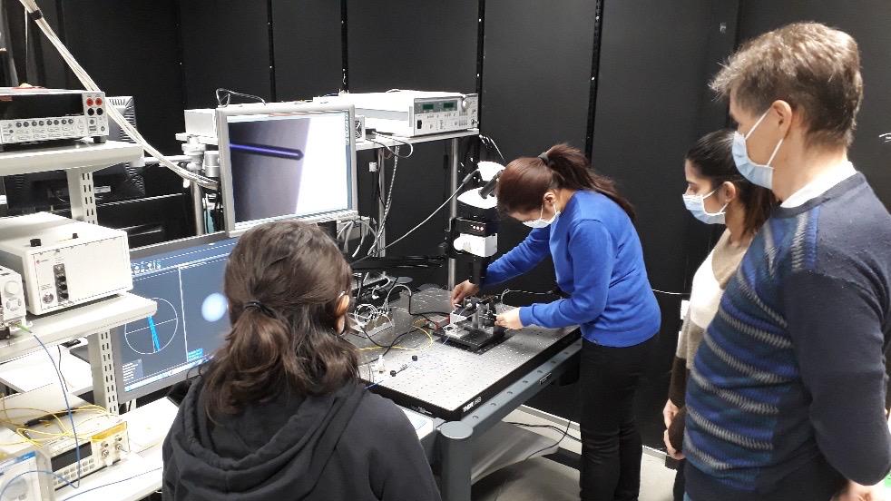
This one-day hands-on training course provides an overview of the Thick-SOI PIC platform and its feasibility in sensing and imaging applications. A clean room tour in Micronova offers an overview of the used fabrication methods and facilities. Hands-on training includes 1) the design of 3 µm SOI PICs using PIC design software, 2) a tour in the clean room and 3) PIC testing in the photonics measurement lab. The last part includes semi-automated fiber-to-waveguide alignment, optical beam steering with an optical phased array (OPA) and testing of silicon photonic chips.

Target audience:
It is desirable but not essential that course attendees have a basic understanding of photonics. The course is ideally suited to those planning to develop new photonic products based on low-loss PICs operating within the 1.2-6 µm wavelength range where the thick (µm-scale) SOI waveguides can operate. Training is primarily intended for industrial participants, but also academic participants and students are welcome.
See the PDF slides for the event HERE, and remember to make your registration HERE.
