SENTECH has over thirty years of experience in developing and manufacturing plasma process technology systems and thin film metrology tools for research and development and industrial production worldwide. Our robust systems focus on the etching, deposition, and characterisation of thin films in semiconductor technology, microsystems technology, photovoltaics, nanotechnology, and materials research.

The SENTECH flexible and reliable plasma etch and deposition systems, including atomic layer deposition equipment, support state-of-the-art processes and applications. Our tools and systems are used worldwide for applications in the fields of nanotechnology, micro-optics, sensor technology, photonics, and optoelectronics.
Low-damage etching and coating with the proprietary SENTECH Planar Triple Spiral Antenna (PTSA) inductively coupled plasma (ICP) source enables our customers to manufacture compound semiconductors and semiconductor devices with outstanding sensitivity, scalability, and non-destructive properties.
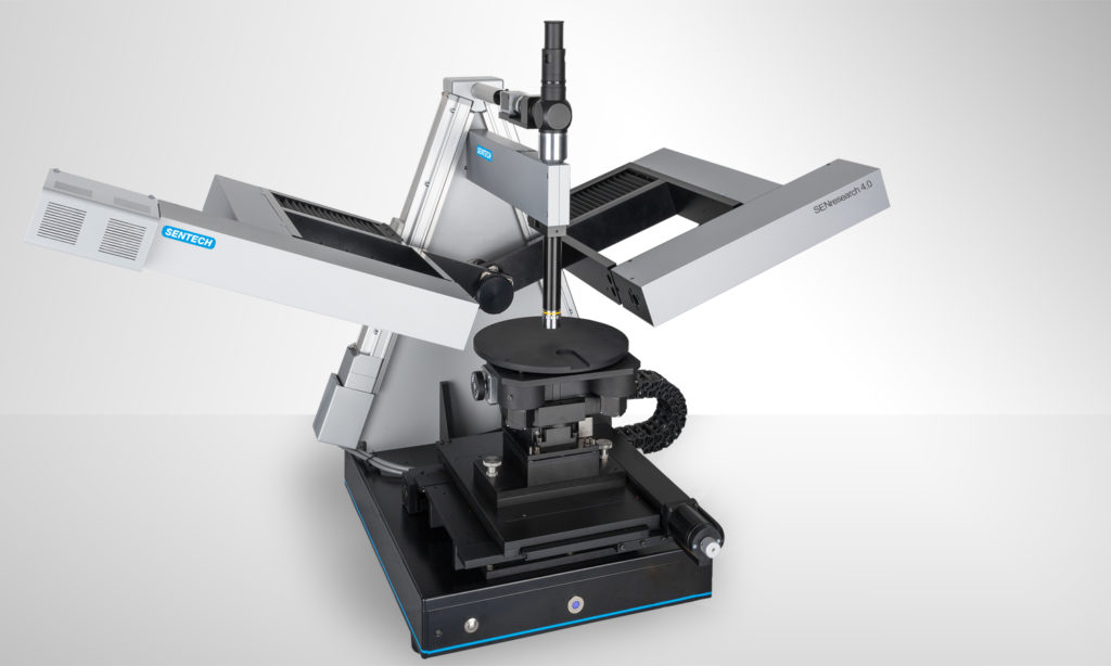
SENTECH offers a wide range of spectroscopic ellipsometers, laser ellipsometers, and reflectometers for measuring the thickness and optical constants of very thin layers or layer stacks. SENTECH has achieved particular success in the field of industrial quality control, for example in photovoltaics, 5G devices, and sensor technology.
For more information or to contact a member of the team, please visit our website www.sentech.de


SENTECH Suomi
Tommi Hietaharju
+358 50 4114118
tommi.hietaharju@sentech.de
Mika Klapuri
+358 40 8485094
mika.klapuri@sentech.de